As with PCB technology, the literature on solder and soldering technologies is extensive and beyond the scope of this volume. The focus of this chapter will be on how the requirements of soldering processes impact on connector design and materials options due to the time/temperature profiles of the soldering processes used. Two different processes, wave and reflow soldering will be briefly discussed.
Wave Soldering
Wave soldering, as the name indicates, is accomplished by passing the component to be soldered across the surface of a literal wave of solder as illustrated in Figure 2.58. Wave soldering is used for Through Hole Technology, THT, as indicated by the pins in Figure 2.71. The board must be prepared prior to soldering in two ways. First, the board must have the appropriate coatings at the points to be soldered. For THT this means the coating on the PTH which will, in most cases, be copper or copper plus an organic or tin coating, as noted previously. Second, flux, to facilitate solder wetting, will be applied to the bottom of the board.


A simplified description of the wave soldering process is in order. For this discussion, assume the solder wave is a fountain with solder flowing as indicated by the arrows. The board enters the wave from the left and is held with the bottom of the board below the surface of the undisturbed wave. Under these conditions the solder flows along the bottom of the board displacing the flux and soldering to the copper plating, or reflowing the tin of the PTH annular ring and inside walls of the PTH. The solder wicks up into the PTH and onto the top surface producing a solder fillet on the top and bottom annular ring. This solder filled hole supports the pins mechanically as well as creating the desired electrical contact condition.
Reflow Soldering
Reflow soldering differs from wave soldering in that the solder must be added to the board and then reflowed through a secondary heating process, while the solder wave provides both the solder and the heat. The solder is applied to the PCB only at pads and lands where device leads are to be soldered to the board. A common means of applying solder is as a screened on paste which contains both the solder and an appropriate flux to facilitate the soldering process.
Reflow soldering is used for Surface Mount Technology (SMT) and hybrid SMT/THT applications. SMT for components other than connectors is more common because of the smaller size of such components compared to connectors and the fact that they do not need to withstand mating/unmating forces. However, SMT compatible connectors have been seeing increasing use in recent years and are now common for pitches below 3 mm.
Several heating processes are used for SMT including Infra Red (IR), IR/convection, and vapor phase. The temperatures and time/temperature profiles for these various processes are different and, therefore, have differing impacts on connector materials and design options. The process temperature is higher, and the time at temperature longer for SMT reflow soldering than they are for wave soldering. This fact places more demanding requirements on the connector housing as will be discussed.


JEDEC standards give important guideline to solder component in the right way. Consider now how these time/temperature profiles impact on the components of a connector.
Contact Finish
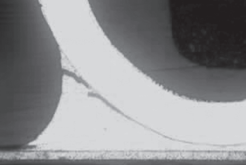
The primary function of the contact finish is to provide, and maintain, the solderability of the connector leads. For the most part this requirement leads to the use of tin coatings on the leads because such coatings are simply reflowed during the soldering process. If the tin is electroplated the quality of the plating process is important. Electroplated tin deposits directly on the surface of the contact whether it is copper alloy, a copper or nickel under plate. The quality of the electroplate becomes important when the tin is reflowed and attempts to form an Intermetallic Compound (IMC) with the contact surface. If the plating quality is inadequate the reflow process may not be able to form IMC uniformly over the contact. If this is the case, the soldering process may result in non wetted or dewetted areas which can compromise the quality of the solder joint between the contact and the PCB pad or land. The potential for dewetting increases as the time at soldering temperature increases. There is a second IMC effect due to time at temperature, excessive IMC growth. IMC tend to be brittle and excessive IMC thickness can lead to a brittle zone between the solder and the pad or contact and compromise the mechanical performance of the solder joint. An example of an IMC related mechanical failure is shown in Figure 2.73. The lead design in this case is a J-lead. The use of a nickel underplate reduces the rate of IMC growth because nickel/tin IMC grows more slowly than copper/tin IMC. Another benefit of nickel underplates comes into play since lead-free solders are required. Nickel underplates reduce the potential for tin whiskering, a concern in lots of applications. Use of contacts with reflowed tin coatings are not susceptible to these IMC and whiskering issues. On the soldering process side, these issues dictate that special attention be paid to minimizing the maximum temperature and time at temperature in reflow soldering.

Contact Spring
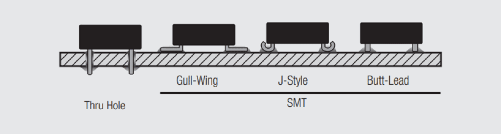
As noted previously, connectors are typically larger than most other SMT compatible components. This means that an SMT compatible connector generally must be attached to the PCB in some fashion to be able to tolerate handling during the reflow process. The design of the contact termination, the permanent connection end of the contact, for SMT applications focuses producing a solder fillet capable of satisfying the mechanical requirements of connector mating and unmating. There are three commonly used geometries, J-lead, gull wing and butt as shown in Figure 2.74. The gull-wing lead is the most suited for connectors because of the larger, and, therefore, stronger solder fillet.

The need to form the terminations of SMT compatible connectors to provide mechanical support introduces an additional issue, termination coplanarity. Coplanarity refers to a requirement that the bases of all the terminations lie on a common plane so that the solder joints of all terminations are acceptable. The solder fillet will depend on the contact between the termination and the solder pad.
There is an additional contact requirement that comes into play during the application lifetime of SMT compatible connectors. The termination end of such contacts must have some compliance to minimize the effects of differential thermal expansion during temperature cycling of the electronic equipment using the connectors. A common source of temperature cycling is the on-off cycling of the electronic equipment. The application ambient temperature will be of the order of 20 degrees Centigrade as will the original temperature of the board mounted connectors in the system. The system temperature will increase as the equipment is powered up, say to 55 degrees Centigrade. This leads to a differential temperature of 35 degrees Centigrade between on and off and, thus a 35 degree thermal cycling exposure.

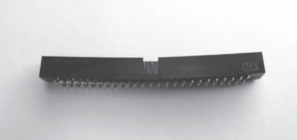
Figure 2.75 shows the curvature introduced into a connector under such a cycle. The Coefficient of Thermal Expansion (CTE) of the FR4 board is less than that of the polymers typically used in connector housings. Therefore, the connector would expand more than the PCB if not fastened to the PCB. Thus, the mounted connector will be under a compressive stress, the contacts will tend to bow towards the center of the connector. The connector/PCB system will return to its original configuration when the equipment is turned off. This produces an opportunity for cyclic fatigue failures of the solder joint. In addition to the fatigue, however, the solder will creep to reduce the stress during each thermal cycle of the system. This process is the most significant degradation mechanism for SMT components, in particular for connectors because, as noted, connectors tend to be larger than other SMT components and the differential CTE effects increase with the length of the component. While the driving forces for CTE cannot be avoided, the stress at the solder joint can be moderated if some of the stress can be accommodated by the contact spring, that is, the compliance of the contact termination to the board can reduce the stresses at the solder joint. The length and thickness (in the direction of expansion) of the contact becomes a design consideration in such cases.
Connector Housing
There are two major effects of SMT time/temperature profiles with respect to the connector housing design/materials. The most significant effect comes from the peak temperature of the soldering process which limits the polymers that are suitable for SMT applications. The second effect is mechanical and arises from the need to fasten the connector to the PCB in some manner to ensure its retention during the handling of the board during the soldering process. Consider the peak temperature effects first.


Simply stated, some of the polymers that are commonly used in connectors, NY66, PBT are not able to withstand the peak temperatures of the reflow soldering process without excessive degradation or distortion. Figure 2.76 dramatically illustrates this statement. The connector shown, in Figure 2.76 uses a polyester as a housing material and has been a reliable performer in the field for many years. After an exposure to a reflow soldering process, however, the housing has severely distorted. Polymers suitable for such soldering processes includes Liquid Crystal Polymers (LCP), PolyPhenyleneSulfide (PPS), Nylon 6T (NY6T), Nylon9T (NY9T). In addition to their high temperature properties, these materials have low moisture absorption and can be molded in thin wall sections to reduce the thermal mass of the connector and, therefore, the time at temperature during reflow. Nylon 46 is a bit particular and can be rated in between as even if it withstands high temperature, great care must be taken, because of its high moisture sensitivity (too much moisture creating bubbles on plastic surface during reflow).
The mechanical consideration, a retention mechanism to retain the connector on the board, is straight forward and dependent only on the ability to injection mold the desired retention feature components into the connector. One additional comment on the retention feature design is in order. Retention features can reduce the potential for problems due to coplanarity and differential thermal expansion. Coplanarity concerns can be moderated if the retention mechanism can preload the contacts onto the solder pad. Differential thermal expansions concerns can be moderated because the retention mechanism tends to hold the connector in place with the PCB expansion reducing the differential expansion and thus the stress on the solder joints.