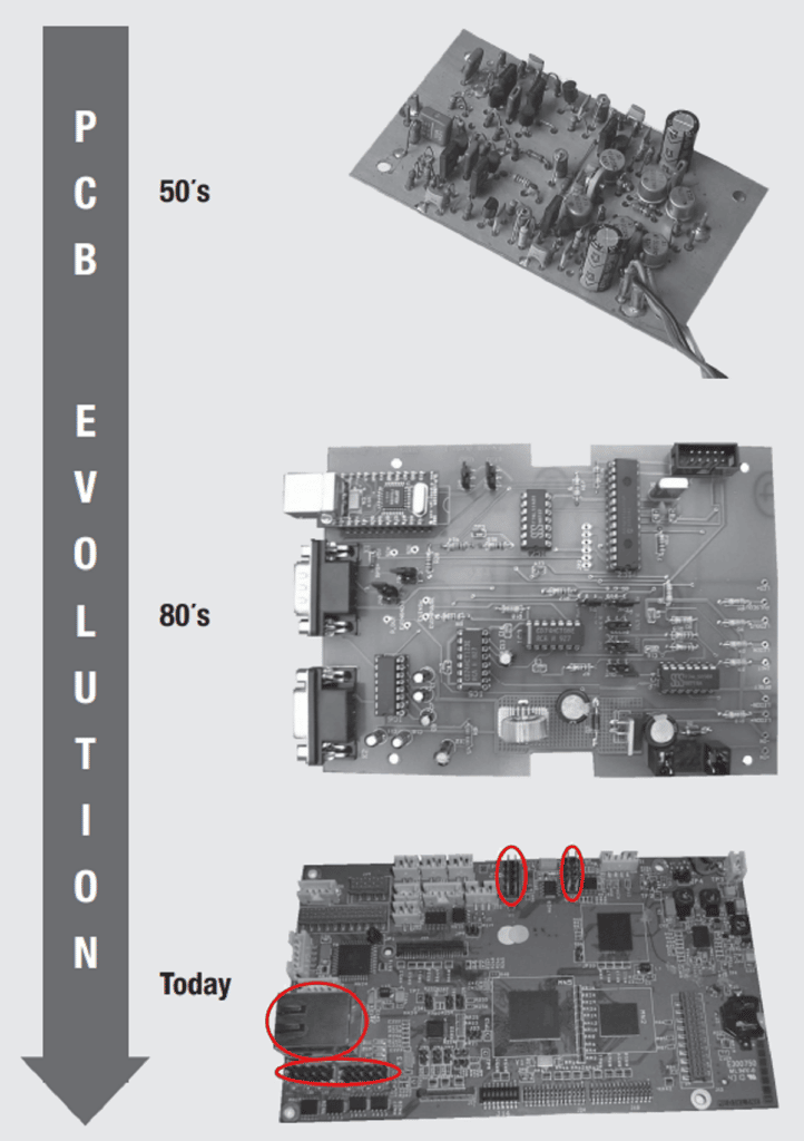
The through-hole technology dates back to the 50’s and was primarily accomplished through wave soldering processes. Components, including connectors, were press-fit into Plated Through Holes (PTH) in a Printed Circuit Board (PCB) and then soldered, generally by wave soldering.
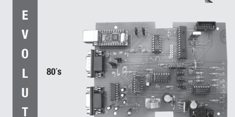
The pioneer work in SMT started in the 60s and had its breakthrough in the 80s. This technology consists in soldering components to lands on the surface of a PCB using a number of different soldering processes. Typically, a solder paste was screened onto the lands on the PCB and the solder paste was subsequently reflowed by a variety of heating processes. SMT capability was originally limited to smaller components and devices, but expanded to include larger components over time. SMT capability brought significant reductions in the PCB size due to reductions in the component size and in the board area required for routing signals. Figure 2.77 illustrates some stages of this evolution.

Initially, connectors were conspicuous by their absence from SMT processing. There were two major reasons for this absence: first, the size of connectors was large compared to that of other SMT components, and second, connectors are subject to mating and unmating forces that exceed the strength capability of the surface solder joints of SMT. This meant that connectors had to be added to a PCB using Through Hole Technology (THT) through compliant pin press-in technologies or through a secondary soldering process e.g. manual or wave soldering.
Eventually SMT versions of smaller connectors were developed. In recent years, however, Through Hole Reflow (THR) or Pin In Paste (PIP) processes have been developed that allow connectors to be reflow soldered in the same soldering process as the SMT components on the board. THR processing results in significant reductions in manufacturing costs as well as in additional savings in PCB board area.


