Researchers from Beijing University of Chemical Technology demonstrated filtering cable with patterned (defected) conductive layer that enables to achieve distributed filtering advantages along its axis.
Abstract
Electrical cables, often referred to as ‘blood vessels’ and ‘nerves’ of the industry, play a vital role in the connection of electrical devices. However, traditional cables that lack distributed filtering functions are usually the primary coupling path for electromagnetic compatibility (EMC) problems.
An innovative design for a filtering cable, which incorporates insulated electrical wires coated with a specific patterned defected conductor layer (DCL), enables it to achieve distributed filtering advantages along its axis.
Microwave network analysis is employed to build the two-port network model of filtering cable, which efficiently analyzes the cascading characteristics of periodic or aperiodic filtering cables.
To validate, the flexible printed circuit board (FPCB) with sawtooth dumbbell-shaped DCL and mounted by capacitors is wrapped around the stripped section of the coaxial cable to manufacture a multi-stopband filtering cable. Simulated and measured results demonstrate that the proposed filtering cable can be effectively suppressed in the stopband, which can be adjusted by changing the values of capacitors.
Introduction
Electrical cables, composed of one or more wires that may be insulated and shielded, play a crucial role in transmitting electrical power or signals between different equipment or modules. They are widely utilized in various industries, earning them the epithets of ‘blood vessels’ and ‘nerves’ of the industrial realm, indicating their indispensable importance in driving global economic advancement.
However, electrical cables, as current-carrying conductors, are usually the coupling path of electromagnetic compatibility (EMC) issues. They may not only conduct electromagnetic interference (EMI), resulting in symptoms of conducted emissions (CE) and conducted susceptibility (CS), but also radiate electromagnetic energy, giving rise to problems with radiated emissions (RE) or radiated susceptibility (RS).
These effects are generally undesirable and can easily lead to electrical equipment malfunction. With the rapid expansion of transformative technologies such as smart grid, next-generation mobile communication, the internet of things, unmanned platforms, and artificial intelligence, traditional electrical cables face significant challenges in terms of EMC.
In order to improve EMC, shielded cables and lumped filters are commonly employed for interconnections within and between equipment. Existing particular cables and filters technologies include shielding, coaxial geometry for achieving electromagnetic shielding with stable impedance and phase, twisted-pair geometry for reducing common-mode interference, flexible microstrip filter transmission line with defected ground structure (DGS), suspension filter circuit, filtering connector, magnetic material filtering, lumped electronic components filters, waveguide filters, ceramic filters, DGS filters, microstrip filters, and various types of filters, etc. However, it is worth noting that, currently there is a lack of distributed filtering functionality along the length of the cable.
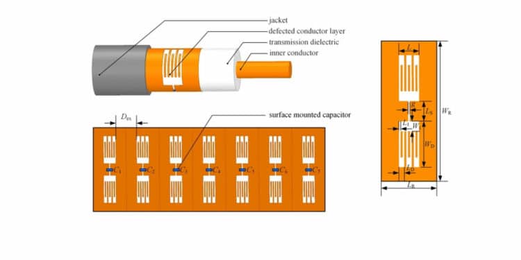
In this work, we present a filtering cable with distributed filtering functions, introduce its design method, and manufacture a multi-stopband filtering cable using sawtooth dumbbell-shaped defected structures (SDDSs) and surface-mounted (SMD) capacitors on a defected conductor layer (DCL) for verification. From a field perspective, the DCL-based filtering cable can be regarded as a waveguide with complex boundaries.
For electromagnetic waves in different frequency bands, a guided traveling wave is formed in the passband and a backward wave is formed in the stopband. The DCL-based filtering cable can be simulated using commercial full-wave simulation software such as HFSS. However, for a long filtering cable, the simulation consumes a large amount of computing resources, which brings great inconvenience to the design.
A more feasible scheme is to obtain the ABCD matrix of each shorter resonant unit of the filtering cable through simulation and calculate the ABCD matrix of the entire filtering cable by cascading the two-port network model of the filtering cable units to achieve the transmission parameters of the entire filtering cable. From a circuit point of view, the defected conductor layer of the DCL-based filtering cable can be converted into a circuit model consisting of capacitors and inductors, incorporated into the cable circuit to suppress EMI signals.
To validate the calculation and simulation method, we conducted a study on a multi-stopband filtering cable that incorporates sawtooth dumbbell-shaped structures on the DCL. Through this study, we can summarize the underlying patterns within its transmission characteristics.
Methods
Filtering cable structure design
By using specific DCL to replace part of the shield of the coaxial cable, a filtering cable with a multi-stopband filtering function can be designed. The DCL manufactured by a FPCB has the advantages of being light, low water absorption, and inexpensive. The SDDS on DCL combined with the capacitor at the gap of the SDDS can make the filtering cable with adjustable band rejection characteristics.
Cascade analysis of two-port network model of filtering cable
On the basis of microwave network analysis theory, a two-port network model of the filtering cable is constructed. When the coupling between filtering cable units is very weak, the S-parameters of a single filtering cable resonator are simulated by full-wave simulation, and the S-parameters of periodic or aperiodic filtering cable cascade structure can be obtained by cascade analysis of the two-port network model, which saves the time of simulating the ultralong filtering cable.
Full-wave simulation and measurement
For the design and simulation of the proposed filtering cable and each of the resonate units, the high frequency structure simulator (HFSS) is used. The S-parameters and radiation of the proposed filtering cables are measured using the Keysight network analyzer (PNA N55524B calibrated by N4691) in the anechoic chamber.
Basic structure design
Illustrated in featured image, the filtering cable featuring a suspended circuit showcases a geometric structure comprising an inner conductor, a transmission dielectric, a defected conductor layer (DCL) with integrated components, and a jacket, arranged from the innermost to the outermost layer. The proposed filtering cable structure bears a resemblance to that of coaxial cables, albeit with a distinguished distinction in the outer shielding layer. Instead of encompassing a complete structure, it showcases meticulously etched patterns and surface-mounted electronic components.
Conclusions
This paper presents a design and implementation method for filtering cable, focusing on a multi-stopband filtering cable example based on the defected conductor layer with sawtooth dumbbell-shaped defected structures and surface mounting capacitors.
The transmission characteristic curves obtained from the two-port network model, full-wave simulation using HFSS, and experimental measurements exhibit a high level of consistency. This validates the applicability of the two-port network model from the microwave network analysis to the design of cascading characteristics for the filtering cable’s resonant units.
The proposed filtering cable cascade model significantly reduces the simulation time required for analyzing the cascading characteristics of the filtering cable’s resonant units. Similar to how a musician composes a beautiful melody using the seven notes of a major scale, engineers can design filtering cables with specific response characteristics by easily adjusting the seven stopbands, following the methodology described in this paper.
Read the full paper:
Han, Y., Xiong, S., Cheng, C. et al. Design of filtering cable with defected conductor layer. Sci Rep 14, 5227 (2024). https://doi.org/10.1038/s41598-024-55736-9


