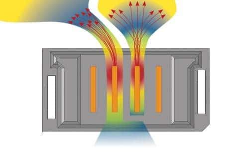
Samtec new connector system improves signal integrity by improving power integrity. Optimizing power integrity provides greater signal integrity margin and improves power and thermal efficiency.
The design of a high-speed connector system’s breakout region, or BOR, impacts signal integrity. The BOR of a power connector also impacts signal integrity. How do we create a BOR that minimizes parasitic inductance?
PI + SI: A New Connector
The featured image above shows Samtec’s new connector system, one that is best in class for both signal integrity performance and power.
It’s the AcceleRate® mP, a combo connector with both signal pins and power blades. The signal pins are rated at 56 Gbps PAM4 performance.
The power blades are rotated 90 degrees in the insulator. This provides up to a 20% increase in current over similar blade-style power systems. It allows a simpler and better path for the current to flow from the board to the connector.
In essence, the BOR of this connector maximizes current capabilities and minimizes distribution resistance in the same form factor. It also reduces current crowding.
With traditional power connectors, the power blades are positioned in line with the width of the insulator. This design increases heat from the adjacent blades and impedes cooling. All of the inner blades are limited to vertical or sideways heat escape, and this leads to current crowding.

The power blades in the AcceleRate mP are in line with the length of the insulator, allowing heat to escape on the broadside of the connector. All blades have equal access to heat escape. This uniform cooling enables a 15% or more increase in current capacity.
Power Integrity: A New Solution
In addition to new connectors like the AcceleRate mP described above, Samtec has a new solution that addresses PI and SI concerns in high-density, high-speed systems.
Today’s AI, server, and switch systems push for extremely high densities and speeds, with a rapidly increasing current demand, in the order of 1,000 Amps. Many systems can benefit from the use of sockets lifting the substrate from the board to allow for testing and accessibility.
In addition, with the advent of co-package optic and copper technologies, packages are getting bigger. They might need to be lifted to provide more real estate for the placement of connectors or a stiffener. In this situation, most, or all of the high-speed signals are routed on the substrate directly. This achieves the best possible SI performance.
Samtec’s new Embedded Capacitor Technology allows designers to elevate the chip off the PCB. Placing bypass capacitors directly on the connector, directly under the load, solves the high-frequency bypass problem. This makes the socket height irrelevant.
This design creates the least amount of parasitic inductance and improves the effectiveness of the bypass capacitors.
This technology can also be used in conjunction with Samtec Flyover® cable technology to optimize the signal integrity performance of the entire system.