
Attention now turns to the effects of a-spots on electrical performance, and, in particular on the electrical resistance the contact interface introduces into the connector. Toaddress that issue requires a discussion of the sources of resistance in a connector.
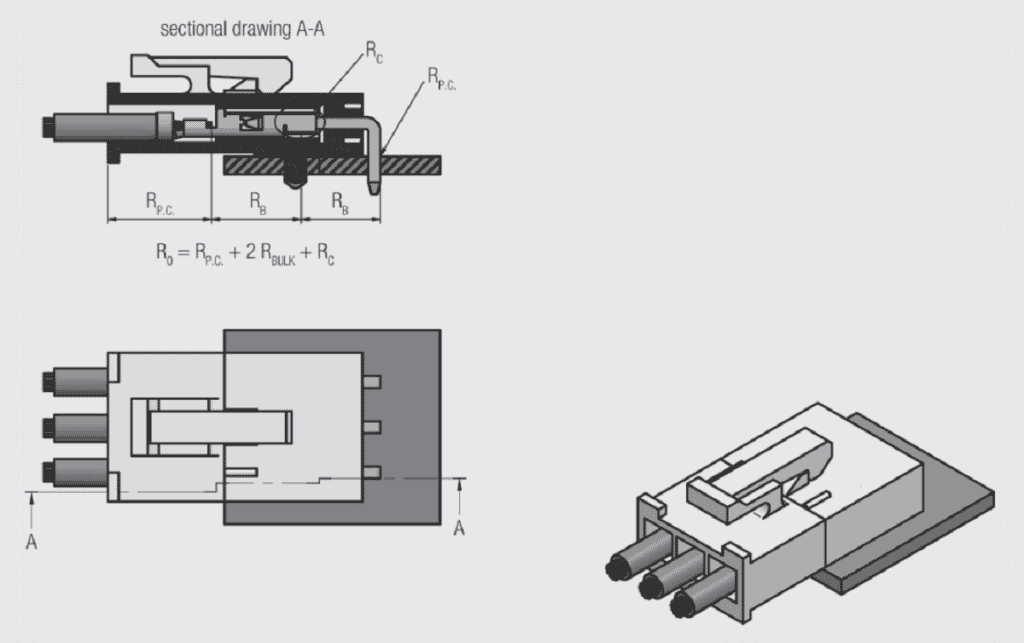
Figure 1.18 shows a cross section of a connector with the various sources of resistance indicated. There are three types of resistances noted. There are two permanent connection resistances RP.C., the resistance of the crimped connection to the incoming conductor and of the pin connection to the plated through hole of the printed circuit board. Permanent connection resistances are dependent on the permanent connection technology used. There are also two bulk resistance contributions RB, from the pin and receptacle contacts individually. Bulk resistances are determined by the resistivity of the material of the contact spring and its geometry. Finally, there is the resistance of the contact interface RC. Only one resistance is cited even though there are two contact interfaces electrically in parallel.

In order to get a perspective on the relative contributions of these three resistances, consider the following thought experiment. If a test probe is inserted through the insulation to the conductor of the wire coming into the crimped connection and a corresponding probe placed in contact with the pad on the plated through hole connection the overall resistance Roverall of the connector can be measured. To provide a benchmark, it is assumed that the connector system shown uses a 0.64 mm (0.025 in) square post. For a connector of this size a reasonable value for the overall resistance is of the order of 20 milliohms. The permanent connections will be less than a milliohm each, the bulk resistances will total about 17 milliohms and the contact resistance will be of the order of a milliohm. Thus, for this connector system the contact interface resistance is of the order of five percent of the overall resistance. Why then is the contact interface resistance so important? The answer is found when the connector system is subjected to a test program to assess its stability under a variety of conditions. If, after such testing, the overall resistance of the connector is measured and found to be, say, 200 milliohms virtually all that change will be in the contact interface resistance.
Bulk resistances are essentially constant. Permanent connection resistances tend to be stable because they have larger contact areas and contact forces than separable interfaces. So, an understanding of the parameters that determine contact interface resistance is critical to knowing how to design and maintain its integrity over the broad range of connector applications and application environments.
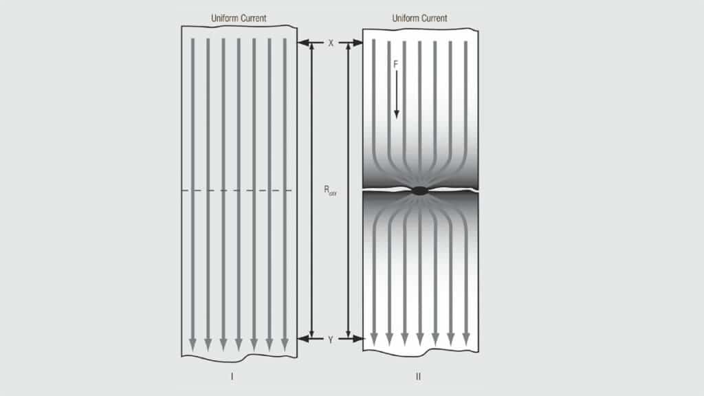
As noted previously, electron flow can only occur through an a-spot, the majority of the apparent contact area is non-conductive. This means that the current distribution through the contacts is constricted to pass through individual a-spots at the contact interface. This geometrical current constriction gives rise to constriction resistance as illustrated in Figure 1.19.

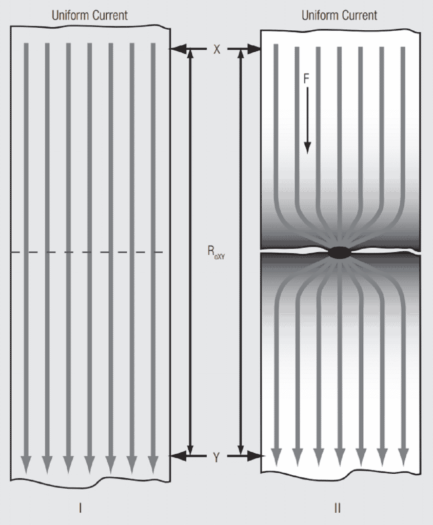
Another thought experiment. The drawing on the left in Figure 1.19 depicts a length of round conductor. Voltage and current probes are connected to the conductor at points X and Y so that a direct current voltage can be applied between points X and Y and the resulting current measured. Ohm’s law, V = I R, where V is the voltage drop, I is the current and R the resistance, can be used to calculate the resistance.
An additional, independent, way to calculate the resistance is using the below relationship: where r is the resistivity of the conductor material, L the length between X and Y and A is the cross sectional area of the conductor. Naturally, these two methods result in the same value of resistance.


Now for the thought part. Assume that a zero thickness blade can be used to cut into the conductor midway between X and Y down to an infinitesimal distance from the center of the conductor. Given that change in conductor configuration the resistance is once again calculated using Ohm’s law. The new calculated value will be much higher than the original value. To explain why we can use our general formula R = r (L/A).
In the original conductor in Figure 1.19 the DC current is indicated by a uniform distribution of current flow lines across the conductor cross section. This, of course, is not what actually happens, but serves as a good visual representation for this discussion. The flow lines are all the same length and distributed uniformly over the conductor cross section.
In the reduced cross section conductor a very different flow pattern exists. If the cut to the center is small enough only one of the flow lines can pass along the conductor unimpeded. All the other flow lines must constrict to flow through the single continuous thread of conductor. This is the source of the term constriction resistance to describe this effect.
Now consider the general formula. Recall that the length of all the flow lines but the central one must increase in length in the new configuration. R is directly proportional to L in the general formula which explains the increase in resistance. Alternatively, note that the current flow lines begin to constrict at some distance away from the reduced cross section. This effect can be modeled by taking a number of slices perpendicular to the axis of the conductor and noting that the cross sectional area of each currentcarrying slice is smaller than the original cross section. R is inversely proportional to A so each of these slices has a higher resistance then the original slice, and all these slices are in series, thus, the increase in resistance.
Note that there is no interface in this model, the conductor is continuous. Constriction resistance is a geometric effect. All contact interfaces will include a number of a-spot interfaces, each of which will introduce a constriction resistance. Thus an interface must produce an increase in resistance to the connector. This resistance can be minimized by maximizing the a-spot contact area, but it cannot be eliminated.

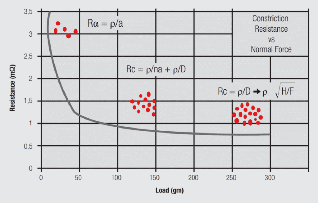
The resistance in Figure 1.20 is the constriction resistance, the resistance of the metal-to-metal contact interfaces. As the plug and receptacle surfaces are brought together under the contact normal force, a few asperity contact interfaces form, as illustrated previously in Figure 1.15, such contacts are referred to as a-spots. The resistance of each individual a-spot, Ra, is given by the formula shown in Figure 1.20:


where ρ is the resistivity of the material, and ad is the diameter of the a-spot. As the force is increased and the surfaces deform against one another additional a-spots are created. The second equation now applies:


Where Rc is the contact interface resistance, n is the number of a-spots in parallel and D is the diameter of the apparent contact area, the area over which the a-spots are distributed at the contact interface. These two resistances are in series because the current constricts first to the dimensions of the apparent contact area, defined by D, and then constricts again to flow through the individual a-spots, defined by ad.
As the contact force continues to increase, the number of a-spots increases along with the apparent contact area. As n increases the a-spot resistance contribution decreases and the contact interface resistance becomes dominated by the resistance due to the apparent contact area. In other words, the interface acts like a single contact area with a diameter determined by the contact geometry.
At this point, the contact resistance can be calculated by the final formula:


where H is the hardness of the contact material and F the contact force. The units of hardness are force/area so the square root of the inverse of hardness gives the diameter of the contact area. This equation shows why the contact force is a fundamental parameter of connector design.