• Latest
  • Trending

Connector Contact Stamping and Forming

September 10, 2022

Webinar PCBs: RIGID.flex with Flexible Soldermask or Coverlay?

September 20, 2023

Samtec Expands with a New Cable and RF Connector Manufacturing Facility in Pennsylvania

September 20, 2023

KYOCERA AVX Unveils New Series Poke-Home Single Contacts

September 20, 2023

Murata Announced Completion of New Plating Research Building in Japan

September 19, 2023

RF Compression-Mount Connectors Enhance Millimeter Wave Designs

September 1, 2023

Würth Elektronik Introduces micro SIM Card Interface with Card Detection

August 31, 2023

Yamaichi Extended Board-to-Cable Connectors for Battery Management

August 15, 2023

How the Connector Blade Assignments Impact Power Integrity 

August 15, 2023

How to Maintain 50 Ohms RF Transmission Path

August 15, 2023

Understanding the Benefits of a Flyover Cable System

July 28, 2023

360° EMC Backshells Enhance the Benefits of the Compact High-Power Harwin Connector Series

July 27, 2023

Molex’s Volfinity Cell Contacting System (CCS) Selected by BMW Group for Next-Gen Electric Vehicle Class

July 25, 2023
  • Privacy Policy
inter-connection blog
  • Home
  • Knowledge base
  • Sister Sites
    • Passive Components Blog
    • PCNS Symposium
    • The Passives Times
    • EPCI Home
  • About
No Result
View All Result
  • Home
  • Knowledge base
  • Sister Sites
    • Passive Components Blog
    • PCNS Symposium
    • The Passives Times
    • EPCI Home
  • About
No Result
View All Result
inter-connection blog
No Result
View All Result

Connector Contact Stamping and Forming

September 10, 2022
A A

Stamping process is used to convert blank metal strip into contacts or shields by cutting and forming it. The press brings the pressure to the die which performs cutting and forming steps.

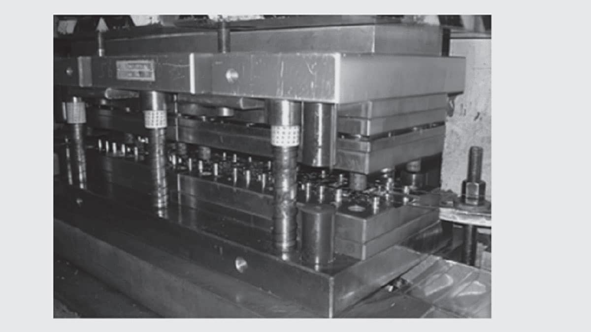
Figure 1.31a illustrates the die into the press, when figure b shows inside the die (in between the two parts). On the c figure we can see the metal strip evolution along the process (from a blank metal strip down to a typical RJ45 metallic shielding)

RelatedPosts

Connectors Explained

KYOCERA AVX IDC RF Shark Fin Connectors for Antennas Vehicle Systems

Binder Launches M12 Panel L-coded Mount Connectors

Fig. 1.31: Stamping progressive die

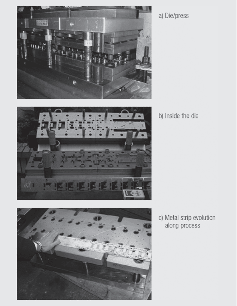
The vast majority of connector contacts are produced by stamping and forming processes using multi station dies that perform a variety of stamping operations including piercing, blanking, shearing and bending among others. The design of the dies and the sequence of the various stations depend on the complexity of the contact design with receptacle contacts being mostly more complex than those of plug contacts.

Related

Source: Wurth elektronik
Next Post

Copper Alloys

Polymer Materials

Polymer Processing

Popular Posts

  • Crimped Connections

    0 shares
    Share 0 Tweet 0
  • THR (Through Hole Reflow) Technology: Introduction & History:

    0 shares
    Share 0 Tweet 0
  • Basic Principles of Connectors

    0 shares
    Share 0 Tweet 0
  • The Electrical Interface: Contact Resistance

    0 shares
    Share 0 Tweet 0
  • Space Saving Molex Connector in AR/VR System designs

    0 shares
    Share 0 Tweet 0

Archive

2023
2022

  • About
  • Inter-Connection Blog
  • Inter-Connection News
  • Knowledge base
  • NEWS
  • Privacy Policy
  • Sister Sites

© 2023 EPCI - Premium Passive Components & Inter-Connect News

No Result
View All Result
  • About
  • Inter-Connection Blog
  • Inter-Connection News
  • Knowledge base
    • Applications
    • Basic Principles of Connectors
    • Design Selection Assembly
  • NEWS
  • Privacy Policy
  • Sister Sites

© 2023 EPCI - Premium Passive Components & Inter-Connect News

This website uses cookies. By continuing to use this website you are giving consent to cookies being used. Visit our Privacy and Cookie Policy.