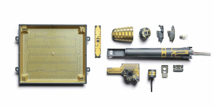
Harting is offering 3D-circuit tracks prints on injection-moulded thermoplastic 3d objects, calling the process ‘3D-Mid’.
The most remarkable aspect of technology is its constant development and improvement. Slimmer laptops, smaller phones, and medical devices designed to be unobtrusive and barely visible to the naked eye. Can I use 3D-Circuits to outperform the flat PCBs?

As electronic devices continue to evolve and shrink, so do their circuits and, ultimately, their components. This development has raised the demand for component miniaturization.
3D-Circuits or also called 3D-MID (three-dimensional mechatronic integrated devices) makes this possible. It allows for more compact designs while enhancing functional density.
Key Benefits of 3D-Mid technology:
- Miniaturisation
- Weight reduction
- Energy savings
- Less heat dissipation
- Integration of mechanical and electrical function into one component
- Better reliability and quality
- The flexibility allows for unlimited design options
- Helps reduce both size and weight
- Shortens assembly time and thus reduces manufacturing costs

“Using 3D-Mid, manufacturers can now design devices that are less invasive and more comfortable for patients, particularly when it comes to monitoring and examining the patient from the inside,” said Harting. “No longer is it necessary to insert a long endoscopic camera down the throat. You can instead consume a non-invasive capsule that contains a little camera that transmits 360° pictures of your body.”


