Electroplating, or electrodeposition, in connector technology refers to the plating of a material, selected for the properties discussed in Chapter I/1.2.3 Contact Finishes, onto a contact spring material, selected for the mechanical and electrical properties discussed in Chapter I/1.2.2 Contact Springs, to optimize the overall electrical performance of the plated contact system.
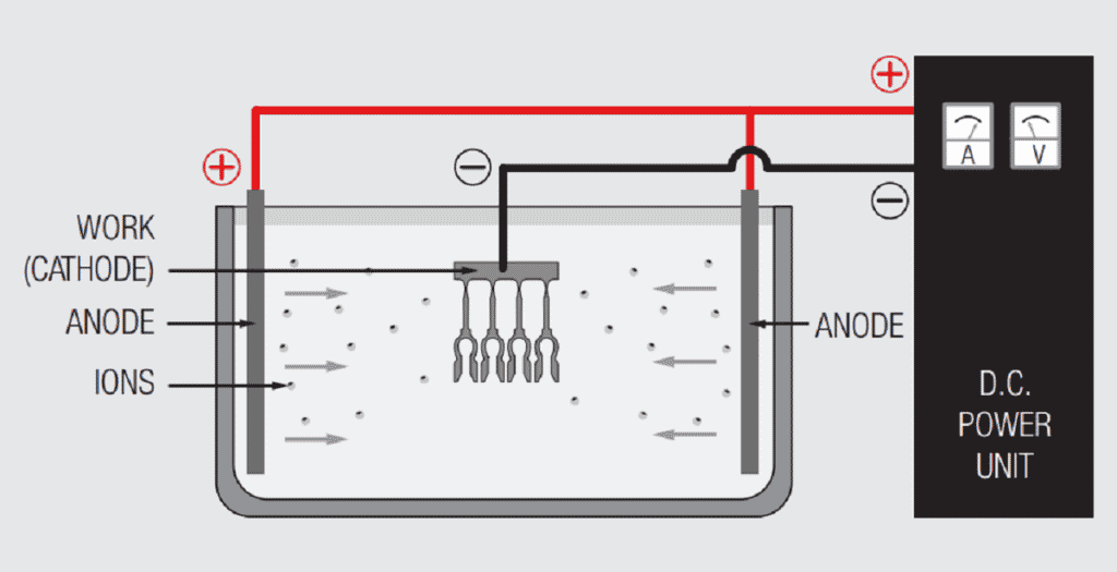
Figure 1.21 schematically illustrates a simple electrochemical plating system. The “electro” part of the system includes the voltage/current source and the electrodes, anode and cathode, immersed in the “chemical” part of the system, the electrolyte or plating bath, with the circuit being completed by the flow of ions from the plating bath to the electrodes. The metal to be deposited may be the anode and be ionized and go into solution in the electrolyte, or come from the composition of the plating bath. Copper, tin, silver and nickel metal usually comes from anodes, while gold salts are usually added to the plating bath in a controlled process to maintain the composition of the bath. The plating bath generally contains other ions to facilitate current flow between the electrodes. The deposition of metal takes place at the cathode.
The overall plating process occurs in the following sequence:
- Power supply pumps electrons into the cathode.
- An electron from the cathode transfers to a positively charged metal ion in the solution and the reduced metal plates onto the cathode.
- Ionic conduction through the plating bath completes the circuit to the anode.
- At the anode two different processes take place depending on whether the anode material is soluble, the source of the metal to be plated, or insoluble, inert. If the anode material is soluble, a metal atom gives up an electron and goes into the solution as a positively charged metal ion replenishing the metal content of the plating bath. If the anode is inert a negatively charged ion from the plating bath gives up an electron to the anode.
- The electron flows from the anode to the power supply completing the circuit.
Note that the deposition of metal at the cathode requires an electron so the rate of deposition depends on the flow of electrons, that is, the current flowing from the rectifier. The thickness of the deposit, therefore, depends on the current and the length of time the current is applied. This relationship is a result of Faraday’s law which relates the weight of a substance produced by an anodic or cathodic electrode reaction during electrolysis as being directly proportional to the quantity of electricity passed through the cell.
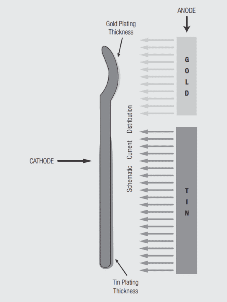
While Faraday’s law fixes the amount of metal deposited, the distribution of that metal is dependent on the distribution of the current. This fact allows for selective deposition of the metal, a process commonly used in connector contact electroplating. Figure 1.22 schematically illustrates the relationship between current distribution and deposited metal thickness. The same amount of current flows in the two geometries so the total metal deposited is the same, but the distribution is very different. The anode and cathode geometries and spacings in connector electroplating practice are designed to shape the current flow between the anode and cathode so as to control the deposition of the finish material, both thickness and distribution, onto the contact. This capability is critical to the successful implementation of selective and duplex plating processes. The sizes, shapes and distance between electrodes are among the proprietary processes of connector electroplating. Plating bath compositions and applied current practices may also be proprietary.