• Latest
  • Trending

Solder Paste Volume

September 12, 2022

Microwave Multi Line Connectors Mounting and Handling Precautions

March 27, 2023

Samtec New Interconnects Enhances Power and Signal Integrity

March 21, 2023
PCNS Passive Components Symposium 11-14th September 2023

PCB Via Design Selection; Plugging-Filling-Tenting

March 20, 2023

Lemo Releases New Multi Coaxial High Frequency Connector

March 2, 2023

Würth Elektronik Introduces Crimp SKEDD Connectors

March 1, 2023

binder Offers Sensor Connectors in Stainless-Steel to Protect Against Corrosion

March 1, 2023

Board-to-Board Connection & Antennas HF Connection

February 20, 2023

How to Ensure Board-to-Board Connectors Meet High-Speed Automotive Assembly and Use Requirements

February 16, 2023

Amphenol Enhanced its ePower-Lite EV Line to Include 3-Pole Connector

February 15, 2023

BASIC PCB Design Rules – Layout

February 15, 2023

Connector Inrush Current Explained

February 3, 2023

M8 Connectors for Smart Farming Applications

January 31, 2023
  • Privacy Policy
inter-connection blog
  • NEWS
  • Knowledge base
  • Sister Sites
    • Passive Components Blog
    • PCNS Symposium
    • The Passives Times
    • EPCI Home
  • About
No Result
View All Result
  • NEWS
  • Knowledge base
  • Sister Sites
    • Passive Components Blog
    • PCNS Symposium
    • The Passives Times
    • EPCI Home
  • About
No Result
View All Result
inter-connection blog
No Result
View All Result

Solder Paste Volume

September 12, 2022
A A

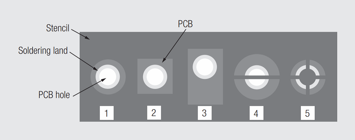
The solder paste volume on the PCB surface will be determined by the thickness and area of the stencil opening. Stencil thickness is in the 100 to 200 micron range, and the area will depend on the PCB design. Typical stencil apertures are shown in Figure 2.88.

Fig. 2.88: Typical stencil apertures

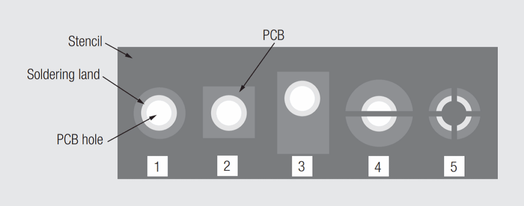
Apertures 1 & 2 are typical for THR printing.
Aperture 3 is used when extra solder paste is needed.
Aperture 4 (paste reducer) is used for large PCB PTHs to prevent the solder paste from dropping through the PTH.
Aperture 5 is commonly used when double printing, top and bottom of the PCB, to add additional solder paste to meet the solder requirement.

Typical PCB pad dimensions are shown in Figure 2.89, where Tb is the PCB thickness, generally 1.6 mm, Dd is the drilled hole diameter (not shown), Dh is the PCB PTH. Dh = Dp + 0.3 mm, where Dp is the pin diameter (shown in Figure 2.89) and Dsp is the solder pad diameter = Dh + 0.5 mm to 0.8 mm.

Fig. 2.89: PCB pad dimensions
Fig. 2.90: Pin diameter

The stencil area, as shown in Figure 2.91, in combination with the stencil thickness (Ts), determines the solder paste volume on the surface of the PCB. Ideally, when an overprint is not necessary, the stencil diameter (Ds ) = Dsp – 0.1 in order to guarantee a perfect paste deposition on the solder pad.

Fig. 2.91: Stencil dimensions

As noted previously, the solder paste consists of approximately 50 percent of the volume of solder particles and 50 percent of the soldering flux volume. The optimum solder particle size depends on the pitch of the PCB pads and on the thickness of the stencil. If the particle size is too large, as per Figure 2.92, the effective solder volume will be reduced.

Fig. 2.92: Effect of the solder particle size on stencil fill

If the solder particle size is too small, viscosity issues may arise, thus affecting the retention of the solder paste in the stencil. The most commonly used solder particle size is in the range of 20 to 45 microns. JEDEC STD-005 covers soldering paste requirements. The pin geometry, square, round or rectangular, may also impact the stencil fill and the solder volume.

Related

Source: Wurth elektronik
Next Post

Solder Paste Application

Pin Geometry

Component Insertion

Popular Posts

  • Crimped Connections

    0 shares
    Share 0 Tweet 0
  • Basic Principles of Connectors

    0 shares
    Share 0 Tweet 0
  • Space Saving Molex Connector in AR/VR System designs

    0 shares
    Share 0 Tweet 0
  • THR (Through Hole Reflow) Technology: Introduction & History:

    0 shares
    Share 0 Tweet 0
  • The Electrical Interface: Contact Resistance

    0 shares
    Share 0 Tweet 0

Archive

2023
2022

  • About
  • Inter-Connection News
  • Knowledge base
  • NEWS
  • Privacy Policy
  • Sister Sites

© 2023 EPCI - Premium Passive Components & Inter-Connect News

No Result
View All Result
  • About
  • Inter-Connection News
  • Knowledge base
    • Applications
    • Basic Principles of Connectors
    • Design Selection Assembly
  • NEWS
  • Privacy Policy
  • Sister Sites

© 2023 EPCI - Premium Passive Components & Inter-Connect News

This website uses cookies. By continuing to use this website you are giving consent to cookies being used. Visit our Privacy and Cookie Policy.