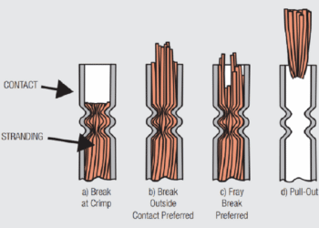
Connectors using noble metal finishes, usually gold, can be used in all applications and environments. Because they are more expensive than connectors of similar designs using non-noble finishes, due to the cost of gold plating, they are not generally used in commercial applications. They are, however, specified in most computer and telecom applications due to their performance advantages.
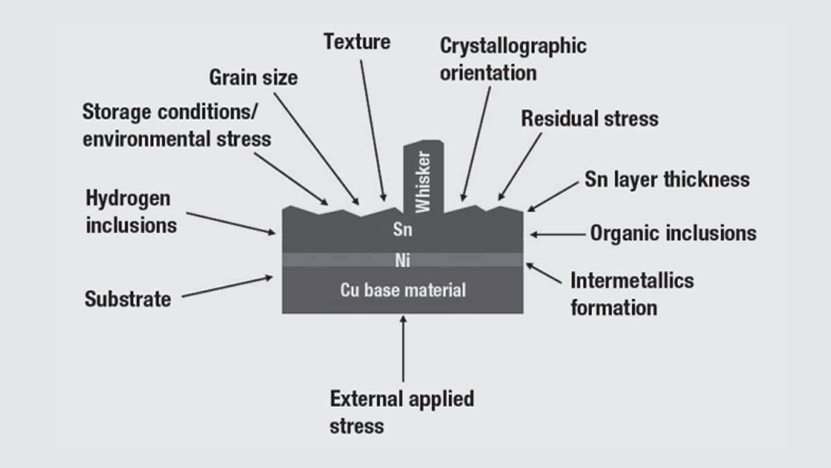
A noble metal contact finish is a system consisting of:
• a noble metal surface, usually gold
• a nickel underplate
• the contact spring base metal (copper alloy)
All three elements influence both the electrical and mechanical characteristics of the contact interface.
Electrically the noble metal surface allows for the formation of the metal-to-metal a-spots that create the electrical contact interface; the nickel underplate provides benefits that protect the nobility of the contact interface due to external corrosion mechanisms; and the constriction resistance takes place in the contact spring material.
Mechanically it is the contact surface that will experience the wear process directly; the hardness of the nickel underplate improves the wear resistance of the system; and the hardness of the base metal contact spring influences the overall amount of deformation that occurs. This effect of the contact spring on deformation is due to the low thickness of the gold and nickel platings, of the order of microns, so that the stresses applied to the contact interface penetrate into the contact spring.
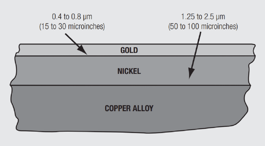
Figure 2.1 schematically illustrates a cross section of a noble metal finish. The noble metal surface plating is usually gold. In computer/telecom applications the gold is typically electroplated to thicknesses of the order of 0.4 to 0.8 µm (15 to 30 microinches). The gold plating used in connectors is typically a “hard” gold. Hard golds are lightly alloyed, 0.1 percent, with cobalt, nickel or iron, with cobalt being the most common. There is an alternative noble metal finish using palladium alloys. The most common palladium alloy is palladium (80)-nickel (20) with palladium (80)-cobalt (20) also used. In this case the bulk of the plating thickness is palladium alloy, but the surface plating may be a gold flash. A flash is a thin plating of the order of a tenth of a micron (4 microinches) in thickness.
The nickel underplate is typically electroplated to thicknesses of 1.25 to 2.5 µm (50 to 100 microinches). Recall from Chapter I/1.2.3 Contact Finishes that the nickel underplate provides several benefits with respect to corrosion and wear which will be discussed in Chapter II/2.1.2 Contact Finish Degradation Mechanisms.
Whisker:
Whiskers are single crystal fibres (when pure Tin plating is used) which can cause electrical failures. Lead was a good way to prevent them as there was no Tin whisker problem while Sn-Pb was the major plating used in the connector industry. Whisker density, length and shape are quite different and unpredictable and can lead to transient or permanent shorts in electric and electronic circuits. Either directly on the component where they have grown or (if they break loose) somewhere else in the circuit.
In the early 2000 years whiskers caused losses of over US$ 1 Billion, mostly in military, satellite and avionic applications, therefore Sn-Pb platings remain active in these fields which are not concerned by the lead free considerations.
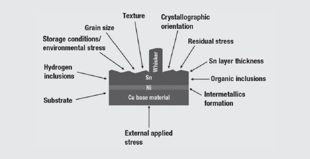
The number of factors and their interactions are so complex that the whisker growth mechanism still hasn’t been totally understood. As it’s not the main purpose of this book to study in details the whisker formation principle, we will only state that it’s mostly connector with small pitches, typically 0.5 mm or lower which are potentially subject to this problem.
In order to prevent Tin whisker creation, the most simple and efficient ways known are to:
• Use another plating than pure tin: like gold (full or selective gold …)
• Use Matt tin instead of bright Tin
• Use Ni under plating below the Tin